- 您现在的位置:买卖IC网 > Sheet目录1230 > MCP6S2XEV (Microchip Technology)BOARD EVALUATION FOR MCP6S2X
�� �
�
�MCP6S2X� Evaluation� Board� (Rev.� 4)� User’s� Guide�
�1.4.5�
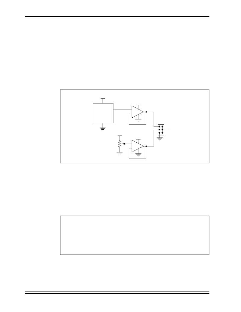
�Reference� Voltage�
�The� MCP6S2X� Evaluation� Board� (Rev.� 4)� has� three� reference-voltage� settings,� as�
�shown� in� Figure� 1-3.� The� MCP1525,� a� precision� reference� voltage� device,� is� used� to�
�provide� a� 2.5V� reference.� The� minimum� supply� voltage� for� this� device� is� 2.7V.�
�Therefore,� this� device� will� not� operate� when� the� evaluation� board� supply� voltage� (V� DD� )�
�is� below� 2.7V.� An� adjustable� reference� voltage� (0V� to� 5V)� is� also� available� using� a�
�mechanical� potentiometer.� Since� the� reference� voltage� input� of� the� PGA� requires� a�
�low-impedance� source,� these� reference� voltages� are� buffered� using� the� MCP6022,� a�
�10� MHz� operational� amplifier.� The� PGA� reference� voltage� input� can� also� be� connected�
�to� ground.� All� of� these� options� can� be� selected� using� the� on-board� jumper� connector�
��Positions”� for� more� information).�
�V� DD�
�MCP1525�
�1/2� MCP6022�
�V� DD�
�+�
�-�
�JP1�
�10� k� ?�
�Pot.�
�V� DD�
�1/2� MCP6022�
�V� DD�
�+�
�-�
�V� REF�
�FIGURE� 1-3:�
�Simplified� Reference� Voltage� Schematic.�
�The� input� and� output� of� this� PGA� can� swing� rail-to-rail� (V� DD� and� GND� supply� voltages).�
�However,� in� order� to� keep� linearity,� the� output� voltage� should� not� exceed� the� Maximum�
�Output� Voltage� Swing,� referred� to� in� the� electrical� specifications� of� the� MCP6S21/2/6/8�
�Data� Sheet� (DS21117).� The� reference� voltage� must� be� adjusted� so� that� the� maximum�
�output� would� not� exceed� the� specified� limit.�
�The� PGA� output� voltage,� with� respect� to� the� input� and� reference� voltages,� can� be�
�determined� using� the� following� equation:�
�EQUATION� 1-1:�
�V� OUT_1� =� G� MCP6S26� (� V� IN_X� –� V� REF� )� +� V� REF�
�V� OUT_2� =� G� MCP6S26� ×� G� MCP6S21� (� V� IN_X� –� V� REF� )� +� V� REF�
�DS51327B-page� 12�
�Where:�
�G� MCP6S26� =� gain� of� 1,� 2,� 4,� 5,� 8,� 10,� 16� or� 32� V/V�
�G� MCP6S21� =� gain� of� 1,� 2,� 4,� 5,� 8,� 10,� 16� or� 32� V/V�
�V� IN_X� =� signal� at� the� MCP6S26’s� selected� channel�
�V� REF� =� Reference� Voltage� at� V� REF� pin.�
�?� 2004� Microchip� Technology� Inc.�
�发布紧急采购,3分钟左右您将得到回复。
相关PDF资料
MCP6XXXDM-FLTR
KIT DEMO BOARD ACTIVE FILTER
MCP6XXXEV-AMP1
BOARD AMPLIFIER EVAL 1 MCP6XXX
MCP6XXXEV-AMP2
BOARD AMPLIFIER EVAL 2 MCP6XXX
MCP6XXXEV-AMP3
BOARD AMPLIFIER EVAL 3 MCP6XXX
MCP6XXXEV-AMP4
BOARD AMPLIFIER EVAL 4 MCP6XXX
MCP73113EV-1SOVP
BOARD EVAL BATT CHARGER MCP73113
MCP7381XEV
BOARD EVAL FOR MCP7381
MCP7382XEV
KIT EVALUATION FOR MCP7382X
相关代理商/技术参数
MCP6S91-E/MS
功能描述:特殊用途放大器 1-Ch. 10 MHz SPI PGA RoHS:否 制造商:Texas Instruments 通道数量:Single 共模抑制比(最小值): 输入补偿电压: 工作电源电压:3 V to 5.5 V 电源电流:5 mA 最大功率耗散: 最大工作温度:+ 70 C 最小工作温度:- 40 C 安装风格:SMD/SMT 封装 / 箱体:QFN-20 封装:Reel
MCP6S91-E/P
功能描述:特殊用途放大器 1-Ch. 10 MHz SPI PGA RoHS:否 制造商:Texas Instruments 通道数量:Single 共模抑制比(最小值): 输入补偿电压: 工作电源电压:3 V to 5.5 V 电源电流:5 mA 最大功率耗散: 最大工作温度:+ 70 C 最小工作温度:- 40 C 安装风格:SMD/SMT 封装 / 箱体:QFN-20 封装:Reel
MCP6S91-E/SN
功能描述:特殊用途放大器 1-Ch. 10 MHz SPI PGA RoHS:否 制造商:Texas Instruments 通道数量:Single 共模抑制比(最小值): 输入补偿电压: 工作电源电压:3 V to 5.5 V 电源电流:5 mA 最大功率耗散: 最大工作温度:+ 70 C 最小工作温度:- 40 C 安装风格:SMD/SMT 封装 / 箱体:QFN-20 封装:Reel
MCP6S91T-E/MS
功能描述:特殊用途放大器 1-Ch. 10 MHz SPI PGA RoHS:否 制造商:Texas Instruments 通道数量:Single 共模抑制比(最小值): 输入补偿电压: 工作电源电压:3 V to 5.5 V 电源电流:5 mA 最大功率耗散: 最大工作温度:+ 70 C 最小工作温度:- 40 C 安装风格:SMD/SMT 封装 / 箱体:QFN-20 封装:Reel
MCP6S91T-E/SN
功能描述:特殊用途放大器 1-Ch. 10 MHz SPI PGA RoHS:否 制造商:Texas Instruments 通道数量:Single 共模抑制比(最小值): 输入补偿电压: 工作电源电压:3 V to 5.5 V 电源电流:5 mA 最大功率耗散: 最大工作温度:+ 70 C 最小工作温度:- 40 C 安装风格:SMD/SMT 封装 / 箱体:QFN-20 封装:Reel
MCP6S92-E/MS
功能描述:特殊用途放大器 2-Ch. 10 MHz SPI PGA RoHS:否 制造商:Texas Instruments 通道数量:Single 共模抑制比(最小值): 输入补偿电压: 工作电源电压:3 V to 5.5 V 电源电流:5 mA 最大功率耗散: 最大工作温度:+ 70 C 最小工作温度:- 40 C 安装风格:SMD/SMT 封装 / 箱体:QFN-20 封装:Reel
MCP6S92-E/P
功能描述:特殊用途放大器 2-C 10 MHz SPI PGA RoHS:否 制造商:Texas Instruments 通道数量:Single 共模抑制比(最小值): 输入补偿电压: 工作电源电压:3 V to 5.5 V 电源电流:5 mA 最大功率耗散: 最大工作温度:+ 70 C 最小工作温度:- 40 C 安装风格:SMD/SMT 封装 / 箱体:QFN-20 封装:Reel
MCP6S92-E/SN
功能描述:特殊用途放大器 2-C 10 MHz SPI PGA RoHS:否 制造商:Texas Instruments 通道数量:Single 共模抑制比(最小值): 输入补偿电压: 工作电源电压:3 V to 5.5 V 电源电流:5 mA 最大功率耗散: 最大工作温度:+ 70 C 最小工作温度:- 40 C 安装风格:SMD/SMT 封装 / 箱体:QFN-20 封装:Reel